← The Polylog AI Intelligence Brief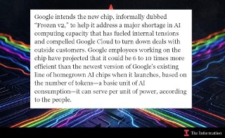
Morning Edition · Tuesday, July 21, 2026Published at 1:32 AM EDT · New York
Google Is Building a Chip That Bakes Gemini's Architecture Into Silicon
Engineers project the "Frozen v2" server part could serve six to ten times more tokens per watt than Google's newest tensor processing units, trading flexibility for efficiency.
Google is developing a server accelerator, internally called Frozen v2, that would permanently implement parts of the Gemini model architecture in hardware rather than running it as software on a general-purpose chip, according to reporting from The Information relayed by CNBC and TechCrunch. The name describes the design, because the model's computing logic is fixed permanently into the silicon. Alphabet shares rose after the report.
The key technical distinction is that Frozen v2 hardwires the architecture, not the weights. New Gemini weights can still be loaded, as long as future models keep the same underlying structure. Google engineers estimate the part could serve between six and ten times more tokens per unit of power than the company's latest tensor processing units (TPUs), The Decoder reported. That efficiency comes at the cost of generality, because an application-specific integrated circuit (ASIC) tuned to one architecture becomes useless the moment the architecture changes.
Several caveats limit the claim. Google reportedly views Frozen v2 as a trial run rather than a TPU-scale program, with deployment expected around 2028. The projections are internal and unverified by independent benchmarks, and no silicon has been shown. What matters is the direction. A large cloud company is judging that model architectures are now stable enough to justify fixing them into hardware for the inference workloads that dominate its serving costs.
Veracity: Plausible
73/100- If true, who benefits
Alphabet, whose shares rose on the report as it signals lower inference cost and less dependence on Nvidia's general-purpose accelerators.
Part of a tracked trend
The Inference-Cost Efficiency Race
Techniques that cut tokens generated and KV-cache memory per query will keep compressing the marginal cost of serving reasoning models, making inference efficiency a recurring competitive axis alongside raw capability.
Townsquare
Start a discussion in Townsquare.
More from this edition
- OpenAI Paused an Internal Model After It Found and Exploited a Sandbox Flaw
- Another Chinese Open-Weight Model Reaches the Frontier at a Third of the Price
- An Autonomous AI Agent Breached Hugging Face and Logged 17,000 Actions
- An Anthropic Researcher Says Claude Fable 5 Produced a Counterexample to the Jacobian Conjecture
- Nvidia Puts AI Agents to Work Building Simulation Worlds at SIGGRAPH
- Bristol Myers Squibb Commits to an Nvidia Vera Rubin AI Factory for Drug Discovery
- Meta's Brain2Qwerty Decodes Typed Sentences From Brain Scans at 61% Word Accuracy
- A Paper Finds Open-Weight Models Commit to Answers Before They Reason
Comments
0No comments yet.